Joined: 30 Dec 2004 Posts: 1179 Location: Tilburg - Netherlands
Posted: Thu Mar 23, 2017 1:33 pm Post subject: UV lasering of photosensitive printed circuit boards
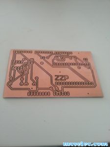
In the Dutch and German Elektor an article about UV lasering of photosensitive printed circuit boards. Edition of Jan/Feb 2017.
Instead of making a film and expose the printed circuit board with an UV lamp, a 500 mW laser is used.
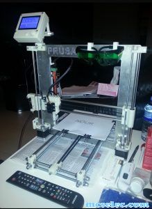
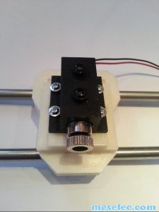
On this page, still in progress, some details about the Eagle to Laser Engraver converter. How to modify your Prusa I3 3D printer for laser engraving, and some real examples of finished boards.
awesome
wish i had this 25 years ago.
Also better for the environment.
As always, great projects !
I still remember my first pcb experiments where i was unaware (it was nowhere mentioned) that there was a black protective layer on the pcb. i was thinking that this layer was the photo layer and it took me some time to find out i had to pull it off. _________________ Mark
You cannot post new topics in this forum You cannot reply to topics in this forum You cannot edit your posts in this forum You cannot delete your posts in this forum You cannot vote in polls in this forum You cannot attach files in this forum You cannot download files in this forum