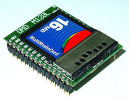
M128LM CPU Module - ATmega128 / 128Kb Ram / 128kB Dflash and MMC connector
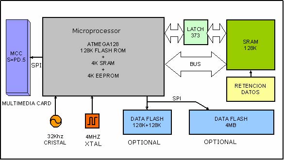
M128LM is a modern microcontroller with low power consumption and small size, based on an Atmel ATmega128L from the AVR family. It also contains a 128Kb static ram and the necessary circuitry for data retention using either a 3V Lithium battery or a Supercap condenser. Some models include a pair of 128KB Dataflash memories (Atmel AT45DB011), adding 256kb of data or a4Mb Dataflash memory ( Atmel AT45DB0321), both connected using the SPI bus.An optional socket on the top of the board is available to hold a Multimedia Card with a capacity of between16Mb and 128Mb, also connected using the SPI bus. (The M128LM has it all)
The oscillator is a 4 MHz ceramic resonator. If the micro needs to be run at a different speed, it can be accomplished using the calibrated internal RC oscillator at speeds between 1 and 8 MHz. In addition, the user program can also change the clock speed on the fly. At 4Mhz, the microcontroller can execute a maximum of 4 MIPS, with a good combination of low power consumption and reasonable speed. The typical Vcc power supply is 3V or 3V3, with low enough power consumption for use in portable equipment. In order to use it at 5V, a voltage regulator is needed and in some cases, adapting/ limiting the voltage on the I/O pins will be necessary. It can directly drive an LCD (which requires a Vcc of 5V) using its I/O port pins ( see example circuits which follow). BLOCK DIAGRAM
The goal of the Mega64L/128L family of microcontroller modules is to include large amounts of RAM/Flash memory onboard, to simplifiy the design work for technicians and engineers and allow then to get their product to market sooner and at a reasonable price. For more information on the AVR series of microcontrollers to go to www.atmel.com.
A very interesting feature of this module is the possibility of connecting a Multimedia Card to the SPI bus, equipping it with the power and flexibility of exceptionally large data storage. Combined with the Bascom-Avr compiler and the AVR-DOS library, it can manipulate files in a powerful, simple and familiar surrounding.Port PD.5 serves as the Chip select for the MMC card.
Up to 4 Mb of low-cost DataFlash memory, can be connected to the SPI bus, to add the potential of nonvolatile storage: very valuable to designers. Chip Select is PE.6 (single 128k or 4Mb DataFlash ) and PE.7 (dual 128k DataFlash). Ram memory is paged as two banks of 64k and by adding an external Supercap or a 3V battery, it becomes a non-volatile memory. RAM Chip select: PE.5=0, A16 is PE.2 ( 64k bank select)
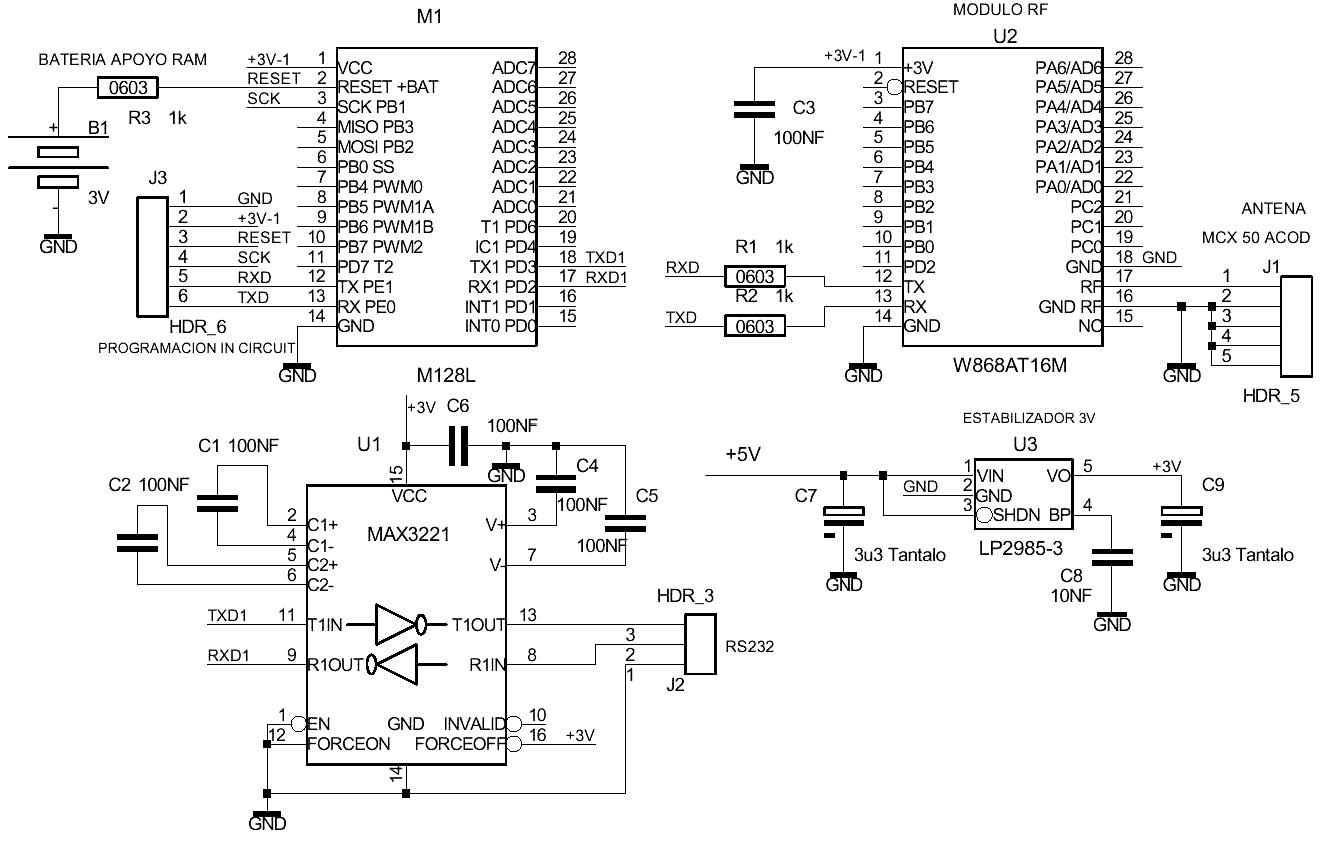
Program loading is done from a PC via the SPI bus using the Atmel AVR-ISP in-system-programing routines. This can be done using a parallel port programmer.. Alternately it can be programmed serially using the onboard bootstrap program (loaded into high Flash memory). Pin 1 of the M128 CPU is the SPI Program Enable pin The built-in Bootloader, (optional) even makes it possible to load programs under internal program control, directly via the serial port. This can be done through either a hard-wired connection or through a wireless RF device like the DMD W868AT16M, Bluetooth, GSM or GPRS. This allows for remote loading of programs which is very desirable for software developers, saving a great amount of time in remote system maintenance. The Bootloader also allows one to copy and load programs from Ram Bank 2 in a maximum of about 4 seconds.
| Num | Name | Denomination |
|---|
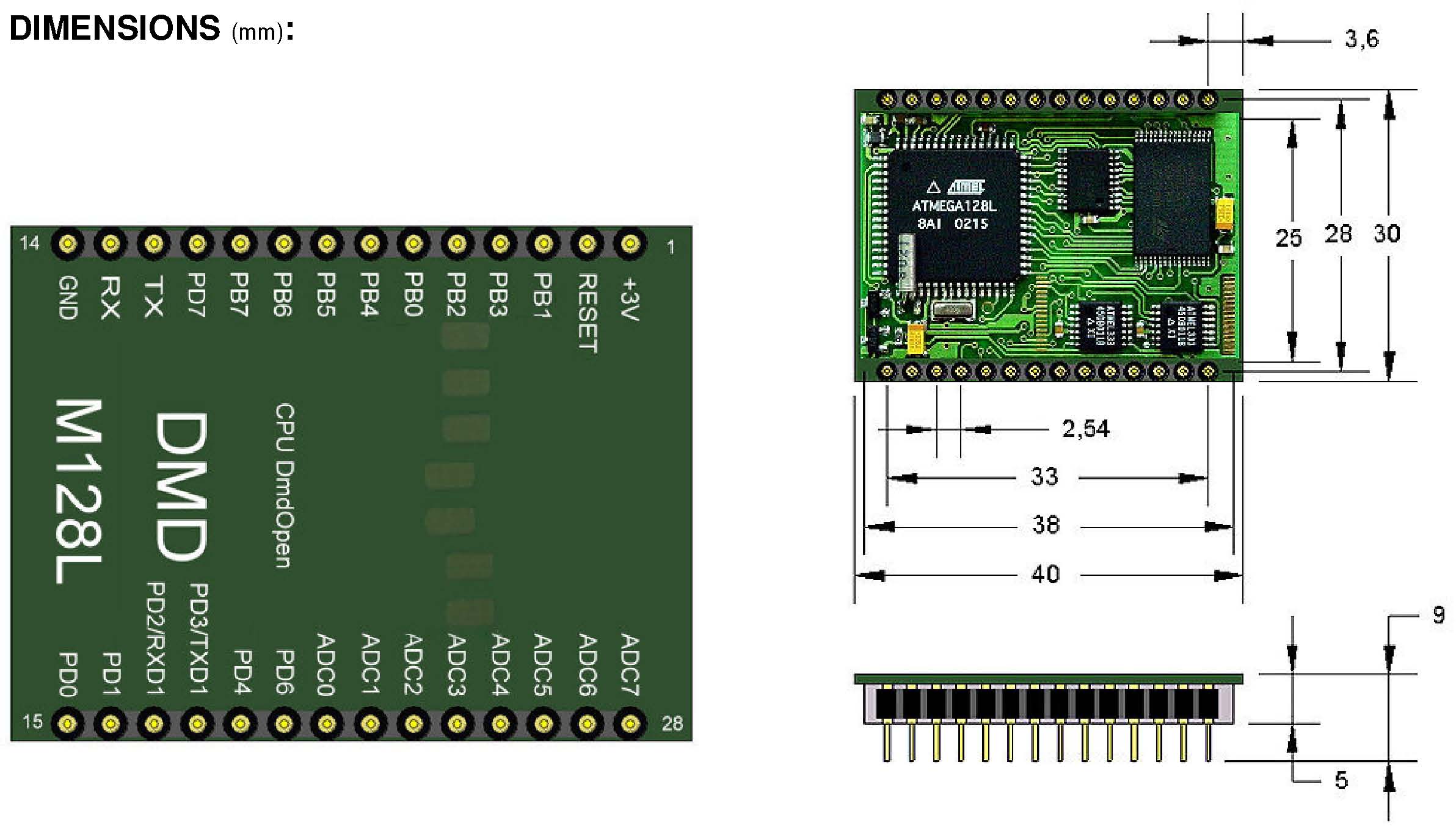
| 1 | VCC | + 3V or +3V3. Regulated power supply. | | 2 | /RESET+BAT | Reset input. A low level for more than 20msec generates a reset. Also connection for 3V Lithium Battery for Sram battery back-up. | | 3 | SCK/PB1 | Port B bit 1. /SCK SPI BUS. | | 4 | MISO/PB3 | Port B bit 3. /MISO SPI BUS. | | 5 | MOSI/PB2 | Port B bit 2. /MOSI SPI BUS. | | 6 | SS/PB0 | Port B bit 0. /Slave Select SPI BUS. | | 7 | PB4/PWM0 | Port B bit 4. /OC0/PWM0. | | 8 | PB5/PWM1A | Port B bit 5. /OC1A/PWM1A. | | 9 | PB6/PWM1B | Port B bit 6. /OC1B/PWM1B. | | 10 | PB7/PWM2 | Port B bit 7. /PWM2. | | 11 | PD7/T2 | Port D bit 7. /T2. | | 12 | TX/PE1 | USART1. Transmit Output (connect to RX of another uC or W868AT16M) /Port E bit 1 | | 13 | RX/PE0 | USART1. Receive Input (connect to TX of another uC or W868AT16M) /Port E bit 0 | | 14 | GND | 0V. Power supply . | | 15 | PD0/INT0 | Port D bit 0. / INT0 interrupt input. | | 16 | PD1/INT1 | Port D bit 1. / INT1 interrupt input. | | 17 | PD2/INT2/RXD1 | Port D bit 2. / INT2 interrupt input /USART2. Receive input | | 18 | PD3/INT3/TXD1 | Port D bit 3. / INT3 interrupt input /USART2. Transmit Output | | 19 | PD4/IC1 | Port D bit 4. /IC1. | | 20 | PD6/T1 | Port D bit 6. /T1. | | 21 | ADC0 | Port F bit 0. Input/output. Analog input 0. | | 22 | ADC1 | Port F bit 1. Input/output. Analog input 1. | | 23 | ADC2 | Port F bit 2. Input/output. Analog input 2. | | 24 | ADC3 | Port F bit 3. Input/output. Analog input 3. | | 25 | ADC4 | Port F bit 4. Input/output. Analog input 4. | | 26 | ADC5 | Port F bit 5. Input/output. Analog input 5. | | 27 | ADC6 | Port F bit 6. Input/output. Analog input 6. | | 28 | ADC7 | Port F bit 7. Input/output. Analog input 7. |
Supply Voltage (Vcc to GND)....................................... -0.5 to +3.7 Volts.
Voltage on any pins except RESET
................................-0.5 to Vcc+0.5.DC
Current per I/O pin
.
.................................. 40 mA.DC
Current Vcc and GND pins
.................................. 200 mA.
Storage temperature.................................................... -25 to +80º C
Operating temperature................................................. -15 to +55º C. Ambient temperature = 20º Celsius Supply Voltage Vcc = 3.0 Volts.
| Power Supply |
|---|
| Supply Voltage | 2.85 | 3.0 | 3.6 | V |
|---|
| Supply Current | 5 | 6 | 10 | mA |
|---|
| Supply Current Vcc and GND pins |
|
| 150 | mA |
|---|
| Time Power On | 64 | 80 | 100 | mS |
|---|
| Suplply Voltaje for reset | 2.6 | 2.7 | 2.8 | V |
|---|
| Dc Current +Bat | 2 | 4 | 5 | uA | For Data Retention |
|---|
| Port Section |
|
|
|
| The sum of IOL, for all ports < 400mA |
|---|
| Input Low Voltage | -0.5 | 0 | 0.3Vcc | V |
|
|---|
| Input High Voltage | 0.6Vcc | 3 | 0.1Vcc | V |
|
|---|
| Output Low Voltage |
|
| 0.5 | V | IOL=10mA, Vcc=3V |
|---|
| Output High Voltage | 2.2 |
|
| V | IOL=-10mA, Vcc=3V |
|---|
| Input Low Leakage Current I/O pin |
|
| 8 | uA | Vcc=3V, pin low (absolute Value) |
|---|
| Input High Leakage Current I/O pin |
|
| 8 | uA | Vcc=3V, pin high (absolute Value) |
|---|
| Reset Pull-Up Resistor | 30 |
| 100 | KΩ |
|
|---|
| Pen Pull-Up Resistor | 25 |
| 100 | KΩ |
|
|---|
| I/O Pin Pull-Up Resistor | 33 |
| 122 | KΩ |
|
|---|
| A/D Section |
|
|
|
|
|
|---|
| A/D resolution |
| 10 |
| Bits | Single Ended conversion |
|---|
| |
| 8 |
| Bits | Differential conversion Gain x1 to x20 |
|---|
| |
| 7 |
| Bits | Differential conversion Gain x200 |
|---|
| A/D Absolute Accuracy |
| 1 |
| LSB | Single Ended conversion |
|---|
| A/D Non-Linearity |
| 0.5 |
| LSB |
|
|---|
| A/D Zero error (offset) |
| 1 |
| LSB |
|
|---|
| A/D Internal Voltage reference |
| 2.56 |
| V | Internal reference |
|---|
| A/D Input Voltage | 0 |
| 2.56 | V |
|
|---|
| A/D Conversion time | 65 |
| 260 | uS |
|
|---|
EXAMPLE: INTERFACE WITH 2X16 LCD DISPLAY: Note: M128L module requires 3V-3V3 and LCD display requires 5V. 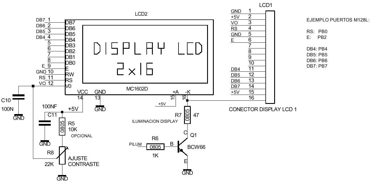
External 128k byte sram: M64L and M128L have a 128K byte static ram memory that can be made nonvolatile connecting a 3V battery (CR2020) or Supercap condensor of 0.5 Farads between GND and the Reset+BAT pin through a 10K resistor. ( this pin is shared with the reset signal, which is also used for ISP program loading via SPI bus.
External 128k byte sram: M64L and M128L have a 128K byte static ram memory that can be made nonvolatile connecting a 3V battery (CR2020) or Supercap condensor of 0.5 Farads between GND and the Reset+BAT pin through a 10K resistor. ( this pin is shared with the reset signal, which is also used for ISP program loading via SPI bus.
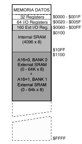
If the application does not require data retention during power interruption, then the battery is not needed. In some cases, when data retention for a few minutes only is sufficient, it can be accomplished using a 470 uF/6.3V condenser or greater connected to the RESET /BAT pin through a 10K resistor ( as in the case of the battery). A 1 to 10K resistor, connected to Vcc, is needed to charge the capacitor. Ram memory is connected to the microcontroller bus through a 373 latch and is addressable as two banks of 64k using port PE.2 as the A16 address line. When PE.2=0,bank 0 is selected. If PE.2=1 bank 1 is selected. Port PE.5 is the sram Chip Select and must be set to 0 to access the sram.. A 1 prevents sram memory access and lowers power consumption.. It is good practice when not using ram, to deselect it, to protect against execution of erratic code by the microcontroller. Note that the first 4K of ram always is located within the microcontrollers internal 4K ram block, so the first 4K of external ram memory will never be written to/read from. This is useful, since swapping data between the two 64K banks requires a buffer if one is using Bascom-AVR without assembly language routines. This internal 4K ram space can be used as this buffer. DataFlash 256k bytes: The M128LDF256 and M64LDF256 modules incorporate two Atmel AT45DB011DataFlash memory chips (128Kb), adding 256k bytes of additional nonvolatile data memory. They are connected to the SPI bus . This bus can also be used to access other external devices, by using different port pins for a Chip Enable for each device. To select one of the two DataFlash memories it, you must assert a 0 on the following port pin. Chip Enable PE.6 selects first 128K DataFlash and PE.7 selects the second 128K DataFlash. These memory devices are also connected to port PE.4: /RST (Reset) and to port PE.3: /WP (Write Protect). For more information see www.atmel.com. DataFlash 4M bytes: The M128LDF4M and M64LDF4M modules incorporate an Atmel AT45DB321 4Mb DataFlash memory chip. It is connected to the SPI bus. In order to select this Dataflash memory, you must assert a 0 on port PE.6, its Chip Enable pin. . This memory is also connected to port PE.4: /RST (Reset) and port PE.3: /WP (Write Protect).
CONSIDERATIONS REGARDING MULTIMEDIA CARD ACCESS: Multimedia Card: The modules contain a socket on the top of the PC board to host a Multimedia card with a capacity of 16, 32, 64 or 128Mbytes. It is connected to the SPI bus. This bus is also used to access the on-board Data Flash as well as optional, external devices, like additional Multimedia cards, by using separate Chip Enable lines for each device. To select the onboard Multimedia Card socket, port PD.5 is used. 
All versions of M64L and M128L allow loading application programs by means of the SPI bus using pins GND, +3V, RESET, SCK, RXD and TXD.
Complete datasheet can be dowloaded here
|


